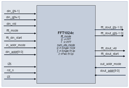
| Name |
I/O |
Width |
Description |
| |
1 |
In |
Clock |
| |
1 |
In |
Active low asynchronous reset |
| clr |
1 |
In |
Active high Synchronous Reset |
| fft_mode |
1 |
In |
0: FFT operation
1: IFFT operation |
| |
2 |
Input |
0 » 1024 point FFT/IFFT operation
1 » 1 512 point FFT/IFFT operation
2 » 2 512 point FFT/IFFT operation
3 » Reserved |
|
|
N |
In |
N bit in-phase input data |
| |
N |
In |
N bit quad-phase input data |
| |
1 |
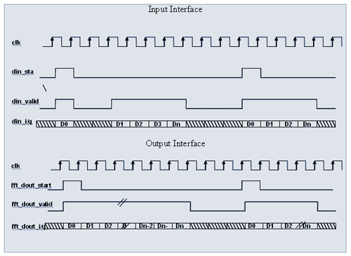
In |
Input Data Valid |
| |
1 |
In |
Start the FFT computation. This signal should be asserted either on the last input data sample or anytime after sending all input data. Internal FFT engine will start FFT computation when fft_din_start is sampled high on the clock edge. FFT output will be available after fixed latency |
| |
1 |
In |
Input Address mode.
1’b0 » Use internal addressing to store input data into the internal buffers.
1’b1 » Use external addressing (din_addr) to store input data into the internal buffers |
| |
10 |
In |
Input address when in_addr_mode is set to 1.
In FFT 512 mode, din_addr[9] is ignored |
| |
1 |
In |
Output Address mode.
1’b0 » Use internal addressing to read the FFT output data from the internal buffers.
1’b1 » Use external addressing (dout_addr) to read the FFT output data from internal buffers |
| |
10 |
IN |
Output address when out_addr_mode is set to 1.
In FFT 512 mode, dout_addr[9] is ignored |
| fft_dout_i |
N |
Out |
N bit in-phase output data |
| fft_dout_q |
N |
Out |
N bit quad-phase output data |
| fft_dout_vld |
1 |
Out |
Output data valid |
| fft_dout_start |
1 |
Out |
Asserted on the first output point of FFT. This signal is asserted after fixed latency from fft_din_start |