| |
 |
| |
Ultra-Compact Advanced Encryption Standard (AES) Core
|
| |
General Description
|
Base Core Features
|
| |
|
The AES core implements
Rijndael cipher encoding and decoding in compliance with the
NIST Advanced Encryption Standard. It processes 128-bit
data blocks with 128-bit key (a 256-bit key version is
available).
Basic core is designed only for encryption and is the
smallest available on the market (less than 3,000 gates). Enhanced versions are
available that support encryption and decryption for
various cipher modes (ECB,CBC, OFB, CFB, CTR), as well
as different datapath widths for size/performance tradeoff. The
core includes the key expansion logic.
The design is fully synchronous and available in both
source and netlist form. |
Encrypts using the AES Rijndael Block Cipher Algorithm.
Satisfies Federal Information Processing Standard
(FIPS) Publication 197 from the US National Institute
of Standards and Technology (NIST). FIPS-197
validated.
Processes 128-bit data blocks with 8, 16 or 32-bit
data interface
Employs key sizes of 128 bits (AES128), 192, or 256
bits (AES256)
Includes the key expansion function
Optional parity check feature
Simple, fully synchronous, reusable design
Completely self-contained: does not require external
memory
Available as fully functional and synthesizable Verilog,
or as a netlist for popular programmable devices and ASIC libraries
Deliverables include test benches
|
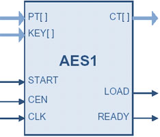
Symbol
|
Applications
|
| |
|
 |
- Cipher for wireless communications, including
IEEE 802.11i, IEEE 802.15.3, IEEE 802.15.4 (Zigbee), MBOA,802.16e,
Wibree, sensor networks ("smart dust"), motes
- Electronic financial transactions
- Power line networks
- Digital Rights Management (DRM)
- Secure video surveillance systems
- Encrypted data storage
- Secure RFID, immobilizers
- Secure Smart Cards
- ITU H.235 VoIP encryption
- Secure RTP (SRTP, RFC 3711)
|
|
| |
Pin Description
|
| |
|
Name
|
Type
|
Description
|
|
CLK
|
Input
|
Core
clock signal |
|
EN
|
Input
|
Synchronous
enable signal. When LOW the core ignores all its inputs
and all its outputs must be ignored. |
|
START
|
Input
|
When
goes HIGH, a cryptographic operation is started |
|
LOAD
|
Output
|
Input
data request signal |
|
READY
|
Output
|
Output
data ready and valid |
|
8-bit Data Interface
|
|
KEY[7:0]
|
Input
|
Encryption
Key |
|
PT[7:0]
|
Input
|
Input
Plain Text Data |
|
CT[7:0]
|
Output
|
Output
Cipher Text Data |
| 16-bit
Data Interface |
| KEY[15:0] |
Input |
Encryption
Key |
| PT[15:0] |
Input |
Input
Plain Text Data |
| CT[15:0] |
Output |
Output
Cipher Text Data |
| 32-bit
Data Interface |
| KEY[31:0] |
Input |
Encryption
Key |
| PT[31:0] |
Input |
Input
Plain Text Data |
| CT[31:0] |
Output |
Output
Cipher Text Data |
|
| |
Function Description
|
| |
An AES encryption operation transforms a 128-bit
block into a block of the same size. The encryption key size
is 128 bit. The key is expanded during cryptographic operations.
The block performs AES encryption as defined in the FIPS-197
http://csrc.nist.gov/publications/fips/fips197/fips-197.pdf
and SP 800-38A
http://csrc.nist.gov/publications/nistpubs/800-38a/sp800-38a.pdf
|
| |
Operation
|
| |
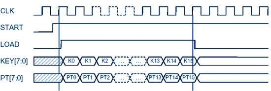
| A rising input on the START port triggers the
beginning of a cryptographic operation on the data PT, using
the KEY as key. The core then raises the LOAD signal requesting
the data block. It then starts to process the state according
to the AES algorithm. The timing diagram below shows how the
data is fed to the core at the start. |
| |
|
|
|
Key and data input at the start
of encryption
|
| |
Both the data and the key are input serially,
8, 16 or 32 bits at the time. The diagram above shows the
case where the input data is 8 bit
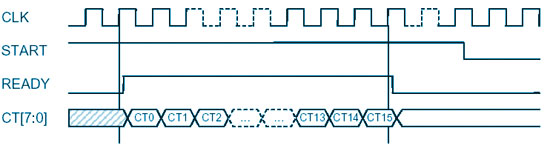
When all the rounds are completed, the READY signal is raised
and the encrypted data starts to flow out. This is shown in
the timing diagram below. |
| |
|
|
|
Cipher text output
|
| |
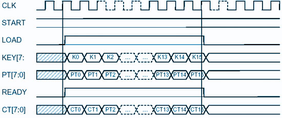
It is possible to start a new cryptographic operation
as soon as the data from the previous one is output. A cryptographic
operation can be aborted at any time by lowering the START
signal for at least one clock cycle.
The core is fully pipelined. Keeping the START signal HIGH
causes the new cryptographic operation to start simultaneously
with ending of previous one; in this case LOAD and READY signals
are generated by the core simultaneously. Loading of the new
plain text data and key is combined with outputting cipher
text data from |
| |
| the previous operation. This is shown in the
timing diagram below. |
| |
|
|
|
Cipher text from a previous operation
is being output while new plaintext is input
|
New key can be used for each cryptographic operation. The
absence of gaps allows sustaining the throughput listed in
the table below. |
| |
|
Core
|
AES1-8
|
AES1-16
|
AES1-32
|
AES1-64
|
AES1-128 |
| Cycles
for 128-bit key |
160
|
80
|
40
|
20
|
10 |
|
Bit per clock cycle
|
|
|
|
|
12.8 |
|
| |
Synthesis Details
|
| |
| The core size starts at less than 3K ASIC
gates. The 128-bit wide core has been synthesized in the
TSMC 90 nm LV process to run at above 800 MHz, delivering 10
Gbps of throughput. Representative area/resources figures are shown below. |
| |
|
Core |
Technology
|
Area / Resources
|
Throughput
bits / clock |
|
AES1-8E |
TSMC 0.18 u
|
2948 gates
|
0.8 |
|
AES1-8E |
Altera FPGA
|
639 ALUT
|
0.8 |
|
AES1-8E |
Actel ProAsic-3
|
864 tiles
|
0.8 |
|
AES1-8E |
Actel RTAX2000 |
3386 cells |
0.8 |
|
AES1-32E/256 |
Xilinx FPGA
|
284 slices
7 BRAM
|
3.2 |
|
AES1-32CBCE |
Actel A3P400 |
18% |
3.2 |
|
AES1-32CBC |
Altera FPGA |
718 ALUT
24576 bits |
3.2 |
|
Please feel free to contact us
for additional synthesis data.
|
Available Versions
|
| |
| The AES core is available in AES-ECB, AES-CFB,
AES-CBC, AES-OFB, AES-OMAC
and AES-CTR modes, for different data path widths, and for key
sizes of 128, 192, and 256 bits. Encryption- and decryption-only
options are also available (identified by E/D). The core
is name is formed in the following way: AES1-<internal
width>[/<external data bus width>][mode][E/D][/key size]. By
default the data bus width is equal to the internal core
width, mode is ECB, core is E+D, and the key size is 128
bits. For example, AES1-32E/256 is an ECB encryption-only
32-bit wide core supporting 256-bit keys, AES1-32CBC is an AES
core implementing the AES-CBC mode. |
| |
Export Permits
|
| |
US Bureau of Industry and Security has assigned
the export control classification number 5E002 to the core.
The core is eligible for the license exception ENC under section
740.17(A) and (B)(1) of the export administration regulations.
See the licensing basics page,
for links to US government sites and more details. |
| |
Deliverables
|
| |
HDL Source Licenses
|
Netlist Licenses
|
| |
|
- Synthesizable Verilog RTL source code
- Testbench (self-checking)
- Test vectors
- Expected results
- Simulation script
- Synthesis script
- User Documentation
|
- Post-synthesis EDIF
- Testbench (self-checking)
- Test vectors
- Expected results
- Place & Route script
- Simulation script
|
|
- NIST FIPS-197 certification (AESAVS) test bench is
available as an option
|
Contact Information
|
| |
|
|