The FFT1024 core implements 1024 or 512 point FFT in hardware. It can be dynamically configured to process one 1024 or two simultaneous 512 point FFT/IFFT operation.
Applications
WIMAX
Communication system
OFDM
UWB
Features
Supports 512 and 1024-point FFT and IFFT and can switch dynamically
Can process up-to two 512 FFT simultaneously (well suited for MIMO application)
Built-in bit reversal. Outputs in Natural order
Supports reading output data in any order (read address)
Low Latency. Can be customized to improve latency vs. gate count
Throughput of 1 sample per clock (0.75 samples per clock for FFT1024-4
Parameterized bit widths and fixed-point option.
Test bench with fixed-point Matlab model
Available in ASIC and FPGA technologies
Minimal gate count implementation
Supports flushing and re-starting the FFT instantly
Configurable bit width based on SQNR requirement for random inputs or for a specific stimuli pattern.
Customization for OFDM applications
Pin Description
Name
I/O
Width
Description
1
In
Clock
1
In
Active low asynchronous reset
clr
1
In
Active high Synchronous Reset
fft_mode
1
In
0: FFT operation
1: IFFT operation
2
Input
0 » 1024 point FFT/IFFT operation
1 » 1 512 point FFT/IFFT operation
2 » 2 512 point FFT/IFFT operation
3 » Reserved
N
In
N bit in-phase input data
N
In
N bit quad-phase input data
1
In
Input Data Valid
1
In
Start the FFT computation. This signal should be asserted either on the last input data sample or anytime after sending all input data. Internal FFT engine will start FFT computation when fft_din_start is sampled high on the clock edge. FFT output will be available after fixed latency
1
In
Input Address mode.
1’b0 » Use internal addressing to store input data into the internal buffers.
1’b1 » Use external addressing (din_addr) to store input data into the internal buffers
10
In
Input address when in_addr_mode is set to 1.
In FFT 512 mode, din_addr[9] is ignored
1
In
Output Address mode.
1’b0 » Use internal addressing to read the FFT output data from the internal buffers.
1’b1 » Use external addressing (dout_addr) to read the FFT output data from internal buffers
10
In
Output address when out_addr_mode is set to 1.
In FFT 512 mode, dout_addr[9] is ignored
fft_dout_i
N
Out
N bit in-phase output data
fft_dout_q
N
Out
N bit quad-phase output data
fft_dout_vld
1
Out
Output data valid
fft_dout_start
1
Out
Asserted on the first output point of FFT. This signal is asserted after fixed latency from fft_din_start
Function Description
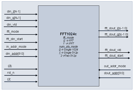
Figure 1. FFT1024c Symbol
FFT1024c can process single stream of 1024 pt FFT/IFFT or 2 streams of 512 pt FFT/IFFT simultaneously.
FFT1024c supports two different modes of input data/output data streaming.
Natural order: In natural order the input buffer addressing is controlled internally. On reset the internal address is set to 0 corresponding to the first fft/ifft input point.
In external address mode, (in_addr_mode ==1), the input data is stored inside internal buffer at the location indicated by din_addr.
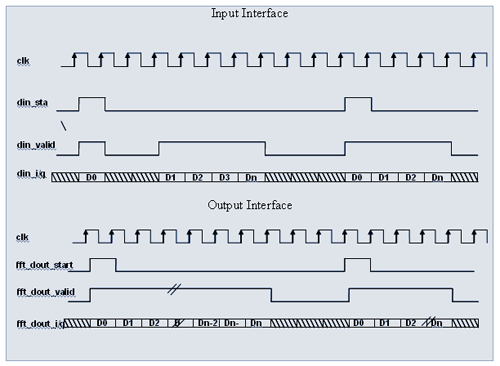
The FFT or IFFT radix operations start when fft_din_start pulse is sampled high. The FFT data output will be streamed out after fixed latency. The fft_dout_start pulse is asserted on the first output data sample.
Similar to input address mode, output address mode can also be controlled internally or externally by providing dout_addr.
Interface timing Diagram
Figure 2. FFT1024c Timing Diagram
Synthesis Details
The 10-bit version of the core size starts at less than 50K ASIC gates. The smaller version of the core (-4) exhibit a latency of 1250 clocks, larger (-8) has 420 clock latency. Ultra-compact (-1) version of the core is also available for MIMO designs with large amount of data streams. Representative area/resources figures for a 10-bit implementation are shown below. All versions of the core require a 1024 x (2 x bit width) x 2 bits of memory.
Configuration
Technology
Area / Resources
Clock
Latency
FFT1024-4-10
TSMC 90 nm
50K gates
250 MHz
1250
FFT1024-8-10
TSMC 90 nm
100K gates
250 MHz
420
FFT1024-4-10
Xilinx Virtex 4
80 MHz
1250
FFT1024-8-10
Xilinx Virtex 4
80 MHz
420
FFT1024-2-16
TSMC 90 nm
18K gates
200 MHz
5200
Export Permits
US Bureau of Industry and Security has assigned the export control classification number 5E002 to the core. The core is eligible for the license exception ENC under section 740.17(A) and (B)(1) of the export administration regulations. See the licensing basics page,
for links to US government sites and more details.
Deliverables
HDL Source Licenses
Synthesizable Verilog RTL source code
Fixed-point Octave(Matlab compatible) model.
Simulation scripts
Self-checking Test environment Test-bench Test-vectors Expected results
Synthesis scripts
User Documentation
Contact Information
IP Cores, Inc.
3731 Middlefield Rd.
Palo Alto, CA 94303, USA
Phone: +1 (650) 815-7996